-
-
-
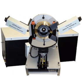
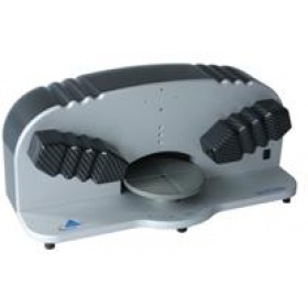
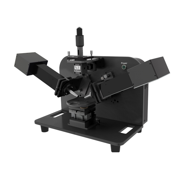
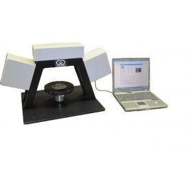
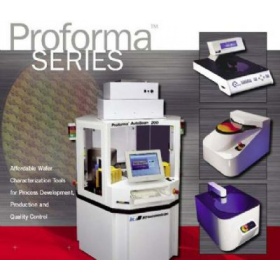
美國(guó)AST橢偏儀

- 品牌:Angstrom Sun
- 型號(hào): SE200BM/SE300BM/SE450BM
- 產(chǎn)地:美洲 美國(guó)
- 供應(yīng)商報(bào)價(jià):面議
-
賽倫科技(北京)有限責(zé)任公司
 更新時(shí)間:2021-04-14 19:14:17
 -
銷售范圍售全國(guó)
入駐年限第10年
營(yíng)業(yè)執(zhí)照已審核
- 同類產(chǎn)品工藝設(shè)備(9件)

立即掃碼咨詢
聯(lián)系方式:400-822-6768
聯(lián)系我們時(shí)請(qǐng)說明在儀器網(wǎng)(www.ghhbs.com.cn)上看到的!
掃 碼 分 享 -
為您推薦
詳細(xì)介紹
美國(guó)賽倫科技為AST在ZG地區(qū)的授權(quán)總銷售服務(wù)商,賽倫科技在上海,北京分別設(shè)有辦事處。
美國(guó)AST (Angstrom Sun Technologies Inc)是世界主要針對(duì)科研單位提供:spectroscopic ellipsometer (SE), spectroscopic reflectometer (SR) and Microspectrophotometer (MSP)的知名供應(yīng)商。
客戶遍布全球主要科研大學(xué)及主要半導(dǎo)體廠商:NIST
ISMI
NASA
JPL
Marshall Space Center
Air Force
MIT
Columbia University
UC Berkeley
Georgia Tech
University of Virginia
USTC,China
...
Bell Laboratories
HP
GE
Lockheed Martin
Corning
Applied Materials
First Solar
Dow Chemical
Samsung
Texas Instruments
National Semiconductor
...
美國(guó)賽倫科技上海辦事處
吳惟雨/Caven Wu Cell:13817915874
QQ:185795008 caven.wu@saratogatek.com
上海市黃浦區(qū)陸家浜路1378號(hào)萬事利大廈產(chǎn)品總述: Functions Spectroscopic
Reflectometer (SR)Microspectrophotometer (MSP) Spectroscopic
Ellipsometer (SE)Wavelength Range 190 to 1700 (or 2300) nm 190 to 1700 (or 2300) nm 190 nm to 30 m Measurable Parameters Film Thickness 20 to 250m 20 to 50m 10 to 10m Optical Constants N & K N & K N & K R/T/A Yes Yes Geometry Yes Digital Imaging Yes Main Features Low Cost, Fast Measurement, Wide Dynamic Range Down to 5 um Spot Size on any Patterned Structure Complicated Layer Stack Options Wavelength Extension, Mapping Stage, Heating/Coo領(lǐng) Stage Unique Options Large Spot Set up for In-Line Metrology Applications Raman & Fluorescence Add-on Set-ups and optional smaller spot size 簡(jiǎn)介:
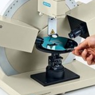
Spectroscopic ellipsometry (SE) is a powerful technique to precisely measure thin film thickness, determine optical constants, investigate surface and interface phenomenon and many other physical, chemical and optical properties of materials. Angstrom Sun Technologies Inc designs and manufactures high quality spectroscopic ellipsometer systems with various options for different applications. Besides ellipsometer system itself, the advanced analysis software is essential to extract the desired information as above-mentioned, such as thickness, roughness, alloy concentration and dielectric constants. TFProbe 3.0from us offers powerful analysis functions for ellipsometry sensitivity study, photometry / ellipsometry simulation and data regression. Unique but configurable mode allows different users to access different level and suitable for both R&D and production quality control purpose.
Models are specified based on wavelength ranges for different applications. The following graph shows available models for standard configurations. In addition, Model 500 simply covers a range of both Model 100 and 400. Customized products are available with wavelength range extension further down to DUV or Infrared (IR) ranges. Normally:
Model 100 covers a wavelength range from DUV to NIR range up to 1100nm.
Model 200 covers DUV and Visible range.
Model 300 covers Visible range, starting from 370nm to 850nm
Model 400 covers NIR range starting from 900nm typically
Model 450 covers Vis to NIR range, starting from 370nm up to 1700nm typically
Model 500 covers DUV to NIR range, up to 2500nm
Model 600 covers NIR to IR range (1.7um to 17um or 1.7um to 30um)
Wavelength range coverage depends on several factors such as light source, detectors, optics used in system, light delivery method (using fibers or not). Because of these factors, all tools can be customized based on specific application. For example, NIR range can be covered up to 1700nm or 2200nm or 2500nm etc. DUV range can be down to 190 nm.
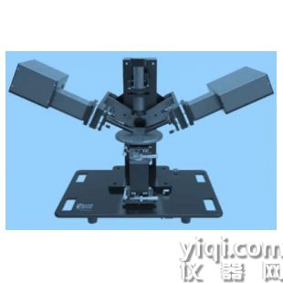
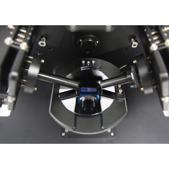
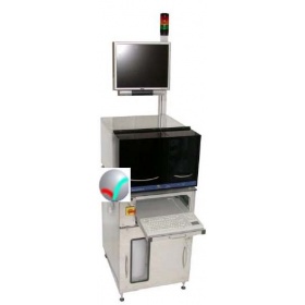
一。SE橢偏儀主要型號(hào) 
==================================
Model SE300BM, 400-1100nm, no mapping,Model SE200BM, 250-1100nm, no mapping
Model SE450BM, 400-1700nm, no mapping
Model SE500BM, 190-1700nm, no mapping
6" stage mapping, adds $20K.
8" stage mapping, adds $22K.
====================================
設(shè)備型號(hào)說明:
Example Model: SE200BA-M300
SE: Spectroscopic Ellipsometer
200: Indicates
B: Detecting Type
A: Scanning monochromator with single element detector
B: Array Type detector with spectrograph or interferometer
A: Variable Incident Angle Type
A: Automatic variable angle with precision Goniometer and computer controlled
M: Manually adjustable incident angle at 5 degree interval
M: Mapping Stage
300: Maximum mapping sample sizeOptions: Wavelength Extension to VUV or IR Range
Stage Size
Probing beam Spot size
Photometry
Heating/Coo領(lǐng) Stage
Mapping stage in X-Y or Rho-Theta
Applications:
Semiconductor fabrication (PR, Oxide, Nitride..)
Liquid crystal display (ITO, PR, Cell gap…..)
Biological films and materials
Optical coatings, TiO2, SiO2, Ta2O5…..
Semiconductor compounds
Functional films in MEMS/MOEMS
Amorphous, nano and crystalline Si
Solar Cell Industry
Medical device fabricationBackground on Ellipsometry:
There are many techniques for characterizing materials, each having its own advantages and disadvantages and each being uniquely able to reveal material properties that other techniques can't access. Spectroscopic ellipsometry (SE) is an optical technique that is particularly flexible in that it can be used to determine the optical and physical properties of a wide variety of thin-film materials. Its ability to do this without contact or damage to the material of interest has seen it become routinely used in R&D laboratories and within manufacturing facilities for monitoring thin film growth and deposition processes.
SE relies on the determination of the polarization state of a beam of polarized light reflected from the sample under characterization. When performing SE measurements, the polarization state is determined at many discrete wavelengths over a broad wavelength range. The change in the polarization state can be traced to the physical properties of the thin film by means of a model. Characteristics such as layer thickness, surface roughness, refractive index (n) and extinction coefficient (k) of the materials can be determined with excellent precision through regression analysis.
The instrument determines two ellipsometry angles Ψ and Δ, which describe the change in the polarization state of the beam upon reflection from the sample. The ratio of the amplitude of the polarization within the plane of incidence (P) to the amplitude of the polarization perpendicular to the plane of incidence (S) is represented by Ψ. The phase retardation between the two polarization vectors P and S is represented by Δ. Changes in Δ and Ψ essentially depend upon the optical constants, n and k, of the layer materials and substrate, physical thickness of the individual layers and surface roughness. A regression analysis allows the determination of these parameters.
SE data for Δ and Ψ are obtained at a number of incident angles in a plane normal to the sample surface and typically at 100-200 different wavelengths for each angle. SE instruments use a white light source and individual wavelengths are selected for detection by either a motor driven monochromator, or a multi-channel detector that can detect many wavelengths simultaneously. Increasing the number of angles and wavelengths at which data are acquired improves analysis precision, especially for complicated epitaxial structures.Note:
1. System configuration and Specifications subject to change without notice
2. * Film property, surface quality and layer stack dependent
3. Customized system available for special applications
4. TFProbe is registered trademark of Angstrom Sun Technologies Inc.
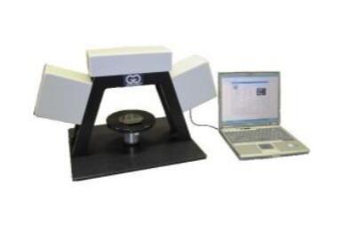
二.Microspectrophotometer(微光斑薄膜測(cè)試儀)MSP100 Microspectrophotometer and Film Thickness Measurement System 
Features
System Configurations
Specifications
Options
Applications
Application Examples
Features:Easy to operate with Window based software
Advanced DUV optics and rugged design for highest uptime and the best system performance
Array based detector system to ensure fast measurement
Affordable, portable and small footprint table top design
Measure film thickness and Refractive Index up to 5 layers over micron size region
Allow to acquire reflection, transmission and absorption spectra in milliseconds
Capable to be used for real time spectra, thickness, refractive index monitoring
System comes with comprehensive optical constants database and library
Advanced Software allows user to use either NK table, dispersion or composite model (EMA) for each individual film
Integrated Vision, spectrum, simulation, film thickness measurement system
Apply to many different type of substrates with different thickness up to 200mm size
Deep ultraviolet light allows to measure film thickness down to 20
2D and 3D output graphics and user friendly data management interface
Advanced Imaging software for dimension measurement such as angle, distance, area, particle counting and more
Various options available to meet special applicationsSystem Configuration:Model: MSP100RTM
Detector: CCD Array with 2048 pixels
Light Source: High power DUV-Visible
Automatic Stage: Black Anodized Aluminum Alloy with 5”x3” net travel distance and 1m resolution, program controlled
Motorized Z focus drive and X-Y-Z joystick
Long Working Distance Objectives: 4x, 10x, 15x(DUV), 50x
Communication: USB
Measurement Type: Reflection/Transmission spectra, Film thickness/refractive index and feature dimensions
Computer: Intel Core 2 Duo Processor with 200GB Hard drive and DVD+RW Burner plus 19” LCD Monitor
Power: 110 240 VAC /50-60Hz, 3 A
Dimension: 16’x16’x18’ (Table top setup)
Weight: 120 lbs total
Warranty: One year labor and partsSpecifications: Wavelength range: 250 to 1000 nm
Wavelength Resolution: 1nm
Spot Size: 100m (4x), 40m (10x), 30m (15x), 8m (50x)
Substrate Size: up to 20mm thick
Measurable thickness range*: 20 to 25 m
Measurement Time: 2 ms minimum
Accuracy*: better than 0.5% (comparing with ellipsometry results for Thermal Oxide sample by using the same optical constants)
Repeatability*: < 2 (1 sigma from 50 thickness readings for 1500 Thermal SiO2 on Si Wafer)Options: TopWavelength extension to to Further DUV or NIR range
Higher power DUV optics for smaller spot size
Customized configuration for special applications
Heating and Coo領(lǐng) Stage for dynamic study
Optional stage size holding samples up to 300mm
Higher wavelength range resolution down to 0.1nm
Various filters for special applications
Add-on accessories for fluorescence measurement
Add-on accessories for Raman applications
Add-on accessories for polarizing applicationsApplications: TopSemiconductor fabrication (PR, Oxide, Nitride..)
Liquid crystal display (ITO, PR, Cell gap…..)
Forensics, Biological films and materials
Inks, Mineralogy, Pigments, Toners
Pharmaceuticals, Medial Devices
Optical coatings, TiO2, SiO2, Ta2O5…..
Semiconductor compounds
Functional films in MEMS/MOEMS
Amorphous, nano and crystalline SiApplication Examples: Top1. Measured Transmission Spectra from Three Filters 
2. Measured Film Thickness
3. Measured Reflection Spectrum over a MEMS Mirror
4. Mapped Thickness Uniformity over 4" wafer
Note:1. System configuration and Specifications subject to change without notice
2. * Film property, surface quality and layer stack dependent
3. Customized system available for special applications
4. TFProbe is registered trademark of Angstrom Sun Technologies Inc.
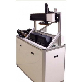
三. SR薄膜反射儀SRM300 Film Thickness Mapping System 
Features
System Configurations
Specifications
Options
Applications
Application Examples
More Information
Features: Film Thickness Measurement - SRM300 Film Thickness Gauge
When you need an accurate thin film thickness measurement our SRM300 allows you to map film thickness and refractive index up to 5 layers thick. No need to worry about complicated equipment since the SRM300 is easy to setup and operate. It uses Windows based software, so most people are already familiar with the look and feel of the operating system. This film thickness gauge can handle various types of geometry substrate up to 300mm in diameter and various types of mapping patterns such as linear, polar, square or even arbitrary coordinates. The array based detector system ensures the fastest film thickness measurement. With its advanced optics and rugged design you can always be sure to get the best system performance.
Easy to set up and operate with Window based software
Various types of geometry substrate up to 300mm in diameter
Various types of mapping pattern such as linear, polar, square or arbitrary coordinates
Advanced optics and rugged design for best system performance
Array based detector system to ensure fast measurement
Map film thickness and Refractive Index up to 5 layers
System comes with comprehensive optical constants database and library
Include commonly used recipes
Advanced TFProbe Software allows user to use either NK table, dispersion or effective media approximation (EMA) for each individual film.
Upgradeable to MSP (Microspectrophotometer) mapping system with pattern recognition, or Large Spot for mapping over patterned or featured structure (with Zonerage Model)
Apply to many different type of substrates with different thickness
2D and 3D output graphics and user friendly data management interface with statistical resultsSystem Configuration:Model: SRM300-300
Detector: CCD Array with 2048 pixels
Light Source: DC regulated Tungsten-Halogen
Light Delivery: Optics
Stage1: Black Anodized Aluminum Alloy Vacuum chuck holds 200 mm wafer
Communication: USB & RS232
Software: TFProbe 2.2M
Measurement Type: Film thickness, reflection spectrum, refractive index
Computer: Intel Core 2 Duo Processor with 200GB Hard drive and DVD+RW Burner plus 19” LCD Monitor
Power: 110 240 VAC /50-60Hz, 3 A
Dimension: 14”(W) x 20”(D) x 14”(H)
Weight: 100 lbs
Warranty: One year labor and partsSpecifications: Wavelength range: 400 to 1050 nm
Spot Size: 500 m to 5mm
Sample Size: 300 mm in diameter
Substrate Size: up to 50mm thick
Number of Layers*: Up to 5 films
Measurable thickness range*: 50 nm to 50 m
Measurement Time: 2ms - 1s /site typical
Positional Repeatability: ~1 m
Accuracy*: better than 0.5% (comparing with ellipsometry results for Thermal Oxide sample by using the same optical constants)
Repeatability*: < 2 (1 sigma from 50 thickness readings at center for 1500 Thermal SiO2 on Si Wafer)
Options: Top Additional Models with Wavelength Extension to DUV or NIR Range: SRM100: 250nm - 1000nm
SRM400: 900nm - 1700nm
SRM500: 400nm - 1700nm
Other Sample Size: 200mm wafer (SRM300-200)
Customized size: Available
Large Spot Accessories for featured structure measurement
Small spot accessories for highly non uniform samples
Applications: TopSemiconductor fabrication (PR, Oxide, Nitride..)
Liquid crystal display (ITO, PR, Cell gap…..)
Biological films and materials
Optical coatings, TiO2, SiO2, Ta2O5…..
Semiconductor compounds
Functional films in MEMS/MOEMS
Amorphous, nano and crystalline SiApplication Examples: Top1. 2D thicknesses plot for Nitride layer in a three layer stack (Nitride-Oxide-Nitride on Glass) 
2. 2D contour plot for Nitride layer in a three layer stack (Nitride-Oxide-Nitride on Glass)
Note:1. System configuration and Specifications subject to change without notice
2. * Film property, surface quality and layer stack dependent
3. Customized system available for special applications
4. TFProbe is registered trademark of Angstrom Sun Technologies Inc.
美國(guó)賽倫科技上海辦事處
吳惟雨/Caven Wu Cell:13817915874
QQ:185795008 caven.wu@saratogatek.com
上海市黃浦區(qū)陸家浜路1378號(hào)萬事利大廈1102室
200011
技術(shù)資料


-
廠商推薦產(chǎn)品
-
 美國(guó)Gaertner激光型橢偏儀,STOKES Ellipsometer
了解詳情
美國(guó)Gaertner激光型橢偏儀,STOKES Ellipsometer
了解詳情
-
 CV儀/汞探針(美國(guó)四維公司)Four Dimensions,Inc.(4D)
了解詳情
CV儀/汞探針(美國(guó)四維公司)Four Dimensions,Inc.(4D)
了解詳情
-
 美國(guó)Mactronix世界Zda的倒片機(jī)/插片機(jī)/分片機(jī)/理片機(jī)生產(chǎn)廠商/光伏太陽(yáng)能行業(yè)/電池片專
了解詳情
美國(guó)Mactronix世界Zda的倒片機(jī)/插片機(jī)/分片機(jī)/理片機(jī)生產(chǎn)廠商/光伏太陽(yáng)能行業(yè)/電池片專
了解詳情
-
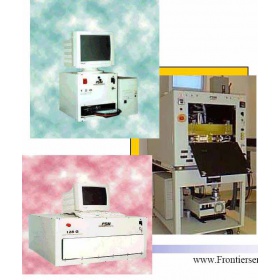 FSM128非接觸薄膜應(yīng)力測(cè)試
了解詳情
FSM128非接觸薄膜應(yīng)力測(cè)試
了解詳情
-
 美國(guó)MTI 測(cè)量硅片幾何參數(shù)(TTV/BOW/WARP/FLATNESS)
了解詳情
美國(guó)MTI 測(cè)量硅片幾何參數(shù)(TTV/BOW/WARP/FLATNESS)
了解詳情
-
 WEP PN深度測(cè)試儀/擴(kuò)散濃度ECV)
了解詳情
WEP PN深度測(cè)試儀/擴(kuò)散濃度ECV)
了解詳情
-